日韩人妻无码一区二区三区久久99-久久精品aⅴ无码中文字字幕重口-香蕉午夜福利院-四虎国产精品永久入口-国产三级片在线观看

Generally, the leakage inductance of the sequential winding method is about 5% of the inductance, but because there is only one contact surface between the primary and secondary, the coupling capacitance is small, and the coupling capacitance is the largest common mode interference conduction path. The interference frequency generated by leakage inductance is relatively low Generally, the leakage inductance of sandwich wound method is about 1-3% of the inductance, but because there are two contact surfaces between the primary and secondary, and the coupling capacitance is large, EMI is difficult to pass. Therefore, for transformers with power below 30-40W, if the leakage inductance energy is acceptable, the sequential winding method is often used; For transformers above 40W, the energy of leakage inductance is large, and generally only the sandwich winding method can be used

Supplementary explanation:

A. Sequential winding method: the primary winding does not cross, winding the primary winding first and then winding the secondary winding or winding the secondary winding first and then winding the primary winding

B. Sandwich winding method: also known as sandwich winding method, that is, the primary or secondary winding is divided into two or more windings for cross winding

C. The leakage inductance of the sequential winding method is generally 5% of the inductance, and the leakage inductance of the sandwich winding method is generally about 1-3% of the inductance (generally calculated as 1.4167%). This value is the design experience value

D. Explain the difference of leakage inductance between the two winding methods from the definition and structural characteristics, as shown in the attachment.

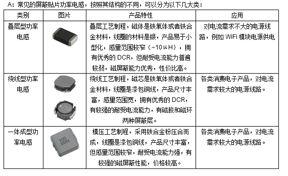
Thermistors are a kind of sensitive elements, which can be divided into positive temperature coefficient thermistors (PTC) and negative temperature coefficient thermistors (NTC) according to different temperature coefficients. The typical characteristic of thermistors is that they are sensitive to temperature and show different resistance values at different temperatures. Positive temperature coefficient thermistor (PTC) has a higher resistance value at higher temperature, while negative temperature coefficient thermistor (NTC) has a lower resistance value at higher temperature. According to different materials, PTC can be divided into ceramic PTC thermistor (CPTC) and polymer PTC thermistor (PPTC). The differences between these types of thermistors are shown in the following table:


category CPTC PPTC Temperature sensing NTC Power NTC
mechanism Nonlinear PTC effect (abrupt/step) Electron level transition
Material Science PTC effect is formed by doping semiconducting elements into BaTiO3, V2O5, BN and other materials Formation of PTC Effect by Adding Carbon Black into Polyethylene Polymers Manganese, cobalt, nickel, copper and other metal oxides are the main materials
Zero power resistance Generally more than 1 Ω, with large loss on the road A few m Ω~a few Ω, low on road loss Class K Ω Grade Ω
electric current Inactive current mA level, applicable to small current protection Inactive current class A, applicable to large current protection Avoid temperature rise caused by self heating and affect temperature measurement. The maximum allowable working current is mA Maximum steady state current Class A
Tolerance High voltage and large current impulse withstand capability is good, and the maximum working voltage is 1KV It is not resistant to high voltage and large current impact, and the maximum working voltage is 600V Do not withstand high voltage and large current impact, Withstand high current impact, not high voltage impact
Action state The action time is relatively slow (hundreds of ms), the recovery time is long, and the recoverability and stability are good after the action The action speed is fast (several ms), the recovery time is short, and the resistance value cannot be restored to the original value after the action Very sensitive to temperature, with rapid thermal response The initial resistance can restrain the transient current in the line. The current increases the temperature of the porcelain body, and the resistance value decreases exponentially. The residual resistance is only m Ω, which has little impact on the overall line
effect Overcurrent protection, overheat protection, motor startup, delayed startup, heating, demagnetization, etc Overcurrent protection Temperature measurement, temperature compensation, temperature protection Suppress transient surge current when starting

The internal electrode of inductor is spiral coil structure, and its equivalent circuit is that the inductance of inductance L0 is connected in series with the resistance of resistance R0, and then connected in parallel with the capacitance of capacitance C0, as shown in the figure below


Wherein, L0 is the inductance generated by the coil; R0 comes from the DC resistance of the coil and the loss generated by the ceramic body (for ceramic inductance, it is mainly the dielectric loss of the ceramic body, which changes with the frequency); C0 includes stray capacitance between coils of each layer; Capacitance between coil and terminal electrode; Capacitance between coil and ground. It is calculated that the equivalent inductance of the inductor is: when the inductor is tested according to different placement directions, the position state of the coil electrode of the inductor and the ground is different, resulting in different capacitance between the coil and the ground. Therefore, the equivalent inductance of the inductor is different


In practical applications, inductors are also affected by peripheral devices. For example, the magnetic flux generated by peripheral devices is coupled to the inductor, causing L0 change; The capacitance between inductor and peripheral devices changes C0, etc. When inductors are placed in different directions, these effects will be different, which will lead to differences in the equivalent inductance of inductors, thus affecting the use of inductors in the circuit.


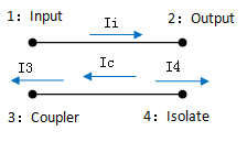
Coupling=10log (P3/P1)


Insertion loss IL=10log (P2/P1)

Isolation=10log (P4/P1)

Directivity=coupling isolation> 0

Ii: current on the straight line

Ic: coupling current

I3: current at coupling end

I4: Current at isolation end

In modern communication, especially in microwave and RF wireless transmission systems, in order to ensure high communication quality, it is often necessary to accurately measure a certain power value, or accurately measure the power value of a certain proportional branch, so that a certain input power can be reasonably allocated to each branch circuit according to a certain specific proportion. In power distribution system: used for signal isolation and mixing In power value transmission system: used for power monitoring and source output stabilization

There is no relationship between dB and dBm< br /> DB is a value representing the relative value, representing the relative size relationship between two quantities, belonging to a dimensionless unit. The calculation formula is 10log (A power/B power)

DBm is a value representing the absolute value of power (it can also be considered as a ratio based on 1mW power), and the calculation formula is 10log (power value/1mw).


If the power P is 1mw, it will be 0dBm after being converted into dBm.


For a power of 40W, the converted value in dBm units shall be:

10log(40W/1mw)=10log(40000)=10log4+10log10000=46dBm。
Definition and formula of standing wave ratio, reflection coefficient and return loss
The standing wave ratio is called voltage standing wave ratio, also known as VSWR or SWR, which refers to the ratio of standing wave belly voltage to wave trough voltage amplitude. When the standing wave ratio is 1, the impedance is completely matched
Reflection coefficient: the matching degree between the load impedance ZL of the transmission line and the characteristic impedance ZC of the transmission line
Return loss is the ratio of reflected wave power and incident wave power at the transmission line port, expressed in logarithmic form, in dB
RL(dB)=10(log(Pi/Pr)

The temperature rise of the product is mainly caused by the heating of the DCR of the product. If the DCR is close, the temperature rise current of the product should have little difference. However, there is no uniform standard for the measurement of temperature rise current in the industry. The standards of each manufacturer are different. The size of the fixture, the contact mode with the product, the heat dissipation capacity of the fixture, and the surrounding environment will affect the temperature rise of the product. The difference of temperature rise current is caused by the disunity of the standards. It is recommended to directly compare the DCR of the product. The smaller the DCR, the better the temperature rise current.

1. The transmission power represents the strength of the wireless signal transmitted by the object to be tested. On the premise of meeting the spectrum template and EVM performance, the higher the power, the better the performance. In practical applications, the larger the wireless coverage, so the transmission power is related to the standing wave ratio and insertion loss. The smaller the standing wave ratio and insertion loss of the filter, the better the transmission power

2. The error vector amplitude [EVM] is defined as the ratio of the root mean square value of the average power of the error vector signal to the root mean square value of the average power of the ideal signal, and is expressed as a percentage. The smaller the EVM, the better the signal quality. EVM is at least related to in band flatness of insertion loss, as well as phase and bandwidth. The smaller the ripple in the filter band, the better the evm. The EVM of digital communication is directly related to the exact position of each constellation point in the constellation diagram. The position of constellation points is nothing more than amplitude and phase The amplitude frequency characteristic of the filter should be flat within the bandwidth concerned, which corresponds to the flatness of the filter's band, that is, ripple The phase frequency characteristic of the filter should be linear within the bandwidth concerned. In fact, the differential between the phase and the frequency is the group delay, that is, the closer the group delay is to a straight line in the band, the better. Of course, the signal-to-noise ratio also affects EVM If the VSWR of the filter is poor, the output power to the transmitter (assumed transmitter) will definitely decrease. The other is that the signal is too large, which will lead to the saturation of the amplifier at the later stage (transmitter part) It will also lead to EVM deterioration. Conclusion: Filter with small ripple and flat group delay should be selected for poor EVM, and filter with small insertion loss and VSWR should be selected for low transmission power.

1. DC resistance of magnetic bead is too large. (Processing: choose magnetic beads with smaller DCR)

2. The magnetic bead impedance is too large, resulting in the filtering of useful signals (processing: select magnetic bead products with low impedance in the signal frequency band)

3. The magnetic permeability of the selected magnetic bead is too high, causing the THD of the signal to be too large (processing: select products with lower magnetic permeability, such as magnetic beads of material K and G).

1) Silver has low resistivity and high conductivity; Copper has high resistivity and low conductivity, and the resistance of copper as electrode is higher than that of silver

2) The co firing characteristics of silver and ceramics are better than that of copper. When different dielectric layers are co fired with conductive silver paste, the reaction and interface diffusion between different interfaces can be better controlled, making the co firing matching of dielectric layers good. The interface layers should be consistent in densification rate, sintering shrinkage rate and thermal expansion rate as far as possible, reducing the generation of defects such as spalling, warping and cracking

3) The melting point of silver is low. The softening temperature of glass powder in the conductive paste used for the internal electrode of LTCC should not be too high; On the other hand, it is not conducive to the fluidity of the sintering process. If the fluidity is poor, the glass body cannot cover the entire screen printing pattern, and the adhesion with the substrate is reduced; To sum up, the process cost of using copper as electrode material is higher than that of silver, and its characteristics are worse than that of silver. Compared with silver, copper is not suitable for electrode material.

It is divided into passive debugging and active debugging

The passive debugging process is as follows:

a. The customer provides more than 1 pcs of optical board for debugging

b. Select the appropriate antenna according to the customer's PCB, debug it to the required frequency band, and provide data including S parameters, smith chart, efficiency and direction chart

The general process of active debugging is as follows:

a. The customer provides debugging objectives and requirements: transmission distance, speed, etc

b. A complete machine that can operate normally, a device that can receive or send signals and match with the whole machine, such as a mobile phone router

c. Refer to the passive debugging data and fine tune the matching circuit to obtain the best antenna performance

d. When fine-tuning the matching circuit, generally change the components in series first, and then change the components in parallel.

Because the antenna application is greatly affected by the surrounding environment, and the layout of different customers is also different, the matching circuit needs to be debugged in actual application. Generally speaking, a pi or L-type matching network will be used for debugging. For specific applications, we will debug the customer's complete machine to the required frequency. In order to facilitate debugging, the antenna will be slightly higher than the required frequency.


Center Frequency: The center frequency at which the antenna is suitable for operation
BW Bandwidth: the frequency range suitable for the antenna to work
Gain: It is an indicator to measure the antenna radiation capacity. The intuitive feeling is that the better the antenna gain of the wireless router is, the WiFi on the first floor can also be found on the second floor
Efficiency: it refers to the ratio of the power radiated by the antenna (i.e. the power effectively converted to the electromagnetic wave part) to the active power input to the antenna. To put it simply, to measure the ability of the antenna to transmit signals, the wireless router on the second floor has a good transmission ability, but whether the first floor can be connected is unknown

A device used to transmit and receive electromagnetic wave signals.

Characteristic impedance is an inherent characteristic of microwave transmission line, which is equal to the ratio of mode voltage to mode current. The characteristic impedance of lossless transmission lines is real, while that of lossy transmission lines is complex. When designing the RF PCB board, we must consider the matching problem, and whether the characteristic impedance of the signal line is equal to the impedance of the connected front and rear components. When they are not equal, reflection will occur, causing distortion and power loss. The above paragraph is a theoretical explanation, which does not need to be understood. You can understand that 50ohm impedance matching is a standard just like 220v mains power. Why is it 220v instead of 210v or 230v? The answer is that this is a standard.

At present, the main recommendation is the frequency divider duplexer, which can be used in the transceiver and connectivity part of mobile phones to distinguish high and low frequency signals, such as GPS and Bluetooth WiFi 1.5G/2.4G signals, or 2.4G/5G WiFi signals. To put it simply, combining two filters into one is a duplexer, while the tripler is a three in one filter, which is used to distinguish 1.5G/2.4G/5G signals.


Center Frequency: the center frequency at which the filter is suitable for operation
BW Bandwidth: the frequency range suitable for filter operation
Insertion Loss: an indicator to measure whether a filter passes a useful signal
Stopband attenuation: an index to measure whether the filter passes through useless signals

A filter is a device or circuit that can process signals. Its main function is to let useful signals pass through without attenuation as much as possible, and to suppress useless signals from attenuation as much as possible. In the filter, the frequency range that the signal can pass through is called passband or passband; On the contrary, the frequency range where the signal is greatly attenuated or completely suppressed is called stopband; The dividing frequency between the passband and stopband is called the cut-off frequency. Our filter is a network composed of multiple inductors and capacitors, mainly divided into low-pass filter, high pass filter and band-pass filter. In short, the filter is to screen out useless signals through useful signals.

HotLine

023 - 4933 9916

WeChat

主站蜘蛛池模板: 成 人 黄 色 网 站 视 频 色| 成人区人妻精品一区二区不卡网站| 黄色网站免费在线观看| 内射少妇一区27p| 亚洲国产精品久久久久爰色欲| 色一情一乱一伦一区二区三区日本| 亚洲精品无码久久久久| 亚欧色一区w666天堂| 国产乡下三级全黄三级| 男人的天堂免费a级毛片无码| 免费观看的a级毛片的网站| 肉蒲团春到肉蒲团冬重燃| 国产自产21区丝袜| 性开放的欧美大片黑白配| 久久久国产精华特点| 国精产品自偷自偷综合下载| 2022国产成人精品视频人| 久久精品国产99国产精品导航| 国产 精品 丝袜| 欧洲熟妇精品视频| 日本少妇寂寞少妇aaa| 国产成人18黄网站| 欧美阿v高清资源在线| 国产精品久久久久久久久免费| 国产成人无码一区二区三区在线| 四虎影在永久在线观看| 在线观看国产成人av天堂| 亚洲国产精品日韩专区av| 国产午夜鲁丝片av无码免费| 老师露双奶头无遮挡挤奶视频| h无码精品动漫在线观看| 久久精品国产99久久久| 成人无码α片在线观看不卡| 奇米影视7777狠狠狠狠色| 人妻少妇无码精品专区| 丰满岳乱妇在线观看中字| 青青青在线视频国产| 欧美大屁股xxxx| 久久国产精品二国产精品| 无码人妻av一区二区三区蜜臀| 久久亚洲av成人出白浆无码国产|